

Musk’s Terafab might be his most technically difficult challenge yet
One does not simply start fabricating semiconductors.
Elon Musk likes to do hard things. Electric cars, reusable rockets, massive data centers, robots — all considered insanely difficult challenges that his businesses have (at least partially) pulled off. But Musks’s ambitious Terafab chip manufacturing project might end up being his most technically difficult challenge yet.
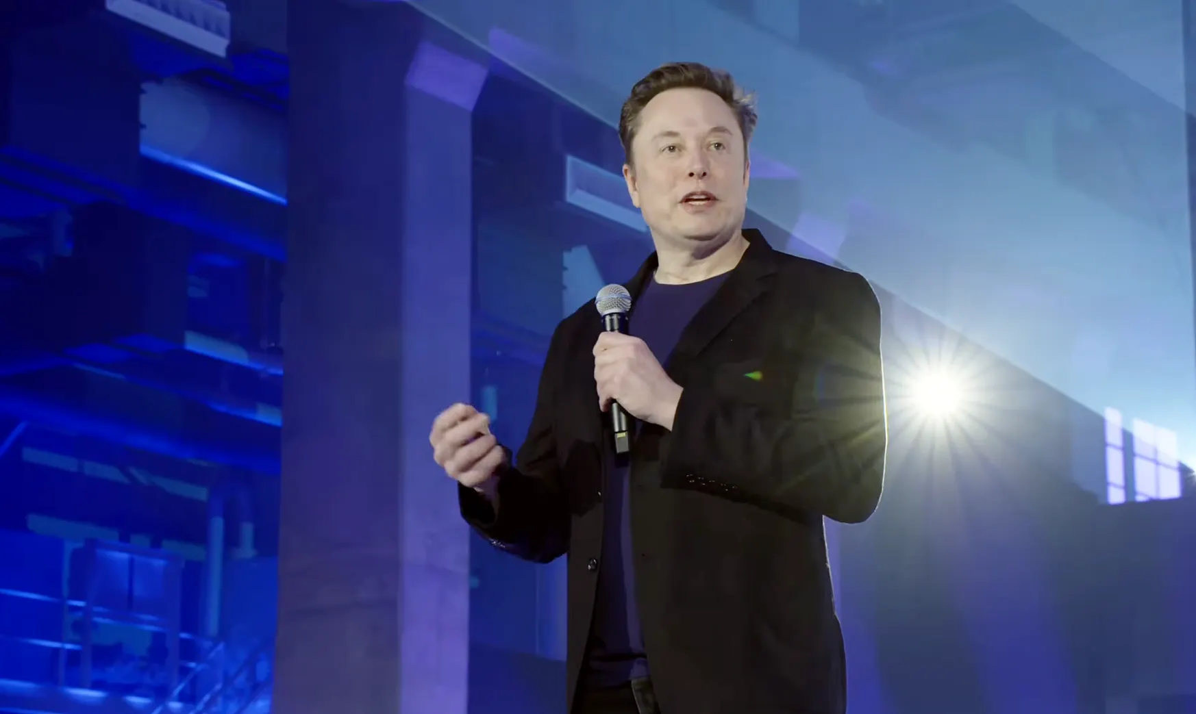
This weekend’s livestream announcing the joint venture between SpaceX, xAI, and Tesla was full of sizzle but light on details. Musk was mainly trying to make the case that his collection of companies are up to the challenge, having “done the impossible before,” listing off the many firsts that those companies had delivered.
Musk outlined a radical vision for rapid innovation for its chip designs, bringing all steps of the complex chip development pipeline under one giant roof:
"So, in the advanced technology fab, we we will have all of the equipment necessary to make a chip of any kind, logic or memory, and we will also have all of the equipment necessary to make the lithography masks. So in a single building we can create a lithography mask, make the chip, test the chip make another mask and have an an incredibly fast recursive loop for improving the chip design. To the best of my knowledge, his doesn't exist anywhere in the world."
But it’s important to note here: one does not simply start fabricating state-of-the-art semiconductors.
Musk had previously said the project is targeting 2 nanometer chips — considered the most densely-packed, advanced chips in the world — but did not mention that target in this event. How could Musk’s Terafab manufacture such advanced chips?
Today there is only one company on Earth that makes the machines that are a crucial step in the process to manufacture such advanced chips — the Netherlands-based ASML. ASML has mastered extreme ultra violet lithography, a technology that allows for etching the smallest and most detailed chip designs on silicon. Chip manufacturing giants like ASML’s biggest customer TSMC use ASML’s EUV machines to build advanced chips for customers like Nvidia and Apple.

While there’s not been any announcement from Musk that his company would buy such advanced equipment from ASML, they’re really the only game in town. ASML’s top-of-the-line Twinscan EXE:5200B reportedly costs up to $380 million apiece and can crank out roughly 175 of the 30-millimeter wafers per hour.
And talk about bottlenecks – ASML sold a grand total of 48 room-sized EUV systems in 2025. The company is seeing huge demand powered by the generative AI boom. It could be a significant wait for Musk to get his hands on the expensive machines, and potentially years before he’s cranking out the billions of chips he wants for powering Tesla’s Optimus robots and self-driving taxis.
The EUV technology is considered crucial not just for the AI boom, but also for national security, which is why China is hard at work trying to replicate the technology. And even a nation state with the vast resources of China has only been able to create a working prototype of an EUV machine, which reportedly takes up an entire factory. And despite this project already being underway, China doesn’t expect to deliver working chips until 2028, at best.
In the Terafab keynote, Musk said that there’s only about 20 gigawatts worth of computing power made every year, and he is expecting that his plans for Tesla and SpaceX will require 1 terawatt of computing each year — 50 times what is made today — which is why he says they need to build the Terafab.
That’s a lot of speculative watts for a group of companies that have not fabricated any of their own chips to date.


